Nano Patterned Thin-Film Optoelectronic Devices
Ray-Photonics is a high-tech manufacturer specializing in micro- and nano-scale optoelectronic components, with full wafer-level mass production capability. Our core competencies include advanced lithography, thin-film deposition, and precision etching, supporting semiconductor packaging, optical devices, sensors, and photonic integration applications
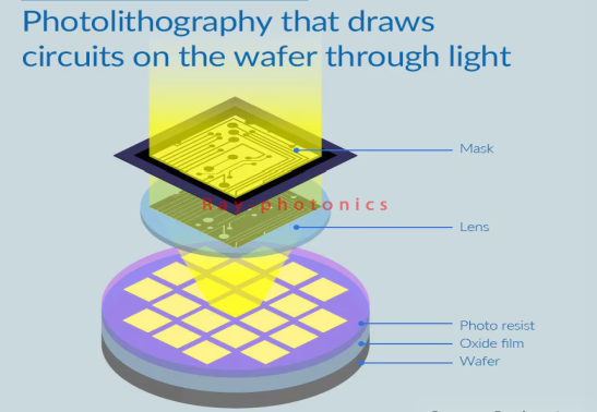
Using advanced micro/nano lithography processes with a minimum feature size of 50 nm, we achieve highly precise and uniform patterning across wafers for optical and semiconductor components.
Wafer-Level Thin-Film Deposition
We provide comprehensive metallization and functional thin-film deposition using magnetron sputtering, IAD, and PECVD technologies. Materials include Au, Ag, Cu, Ni, Cr, Al, Ti, TiW, W, and Zr. Our optical uniformity across 8-inch wafers is within 2%, ensuring reliability for infrared filters, AR coatings, and bandpass filters.
Multi-Process Etching Technology
Our expertise covers both physical (RIE, IBE) and chemical (wet/dry) etching. By flexibly combining processes, we produce complex microstructures, metallized windows, and multilayer thin-film systems with high precision and repeatability.