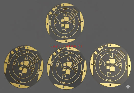
Metallized Ceramic
Metallized Ceramic
Metallized ceramic PCB(AuSn metallization for laser packaging)----Micron-level photolithography mask technology + PVD magnetron sputtering coating machine + electroplating technology


Metallized ceramic PCB(AuSn metallization for laser packaging)----Micron-level photolithography mask technology + PVD magnetron sputtering coating machine + electroplating technology

Aluminum nitride ceramics , Alumina ceramics
Metallized Ceramic Circuit Boards
| Parameter | Unit | Measured Value |
| ALN ,AL2O3,Si3N4 Ceramics | % | ≥99.9 |
| Thermal Conductivity | W/m·K | 29~320 |
| Coefficient of Thermal Expansion | X10⁻⁶/K | 6.9 (40~300℃)<br>7.3 (40~500℃)<br>7.8 (40~800℃)6.9(40~300℃)<br> 7.3(40~500℃)<br> 7.8(40~800℃) |
| Q Value | >10000 | |
| Dielectric Constant | εr | 9.8 @10GHz<br>10.3 @1MHz |
| Standard Material Surface Roughness | As fired: 0.25 μm RaMax.<br>Lapped: 0.30 μm RaMax.<br>Polished: 0.025 μm RaMax. |
Product Overview
Our metallized ceramic circuit boards are manufactured from 99.9% high-purity polished aluminum nitride (AlN). Each substrate undergoes rigorous inspection for surface roughness, flatness, and mechanical stability. Using advanced magnetron sputtering combined with laser trimming technology, we produce planar platinum resistors with excellent reliability. These resistors can replace imported products and, in some applications, provide a cost-effective alternative to NTC thermistors.
Key Features
Custom design solutions available
Single-sided or multilayer metallization (2.5 μm – 10 μm)
Thin-film resistor integration
High-precision circuit processing (line width/spacing down to 3 mil)
Conductor thickness: 0.01 – 0.5 mm
Micro-via filling and hermetic sealing
Inorganic dam ring technology
3D circuit fabrication capability
Electrode Materials
Cu,Ni, Ag, Cr, Ti, TiW, NiV, NiCr, Pt, Au, AuSn
Applications
Metallized electrode films are used in:
Communication antennas
Automotive power modules
AC/DC converters
Ignition systems
Switching regulators
Solid-state relays
Rectifier bridges
Microwave devices
High-power semiconductor lasers
High-frequency components
GET IN TOUCH

